-
PCB多层线路板 HDI堆栈
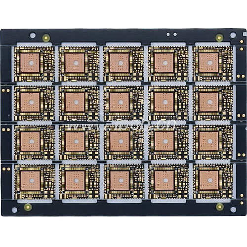
发布时间:2023-10-06 | 信息来源:遇见电路(深圳)有限公司PCB多层线路板初始设计中最重要的方面之一是定义其适当的堆叠。这对于具有多个引脚数BGA的大型,密集的PCB是必不可少的,尤其是当标准层压板堆叠在成本和性能目标方面不足时。HDI堆栈是大量层的可行替代方案,如果设计合理,则可以提供更低的成本和更高的性能。
对于具有高引脚数BGA的电路板,可以有三种类型的堆叠:带通孔的标准层压,带盲孔和掩埋通孔的顺序层压以及带微孔的堆叠。其中,HDI电路板主要使用带有微孔的结构,因为它具有以下优点:
①通孔和走线的特征尺寸较小,从而导致更高的布线密度和更少的层数。
②可以更有效地使用微通孔图案,这将打开更多的布线通道,并可能导致更少的层
③这是设计多个间距小于0.8 mm的大型BGA的实用方法。
④为高密度板提供较低的成本。
⑤适当的堆栈定义可改善信号和电源完整性。
⑥必须满足RoHS标准的工艺所需的适当材料。
⑦可以以较低的成本获得更新的材料以实现更高的性能,但是这些新材料可能不适用于其他类型的覆膜。
有的PCB制造商已经定义了16层HDI PCB叠层,其总板厚仅为66±7mils。这需要顺序堆积(SUB),并具有激光钻孔的微孔。下一篇:影响HDI电路板成本的因素相关资讯

专业高精密PCB电路板研发生产厂家
PCB打样加急,高频线路板,PCB多层线路板,线路板打样,FPC软板打样生产
热线:13798484718 邮箱:445752204@qq.com
