-
深圳高频高速板哪家好
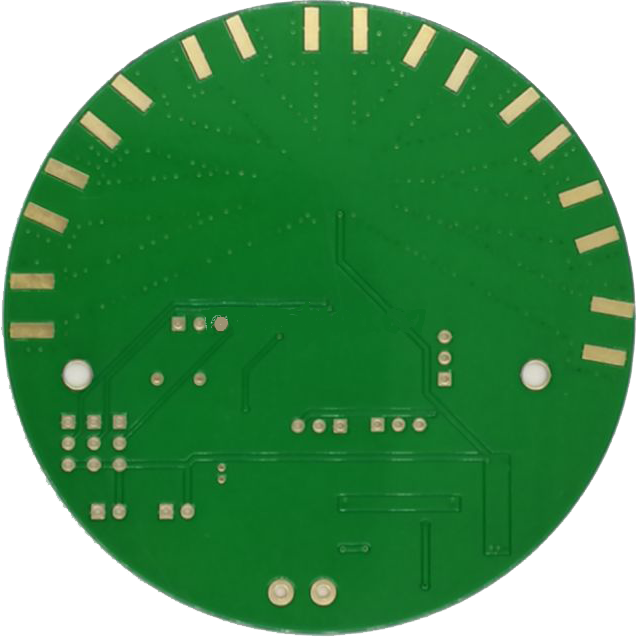
发布时间:2023-10-26 | 信息来源:遇见电路(深圳)有限公司高频高速板随着电子技术的快速发展,印制电路板极广应用于各个领域,几乎所有的电子设备中都包含相应的印制电路板。为保证电子设备正常工作,减少相互间的电磁干扰,降低电磁污染对人类及生态环境的不利影响,电磁兼容设计不容忽视。本文介绍了印制电路板的设计方法和技巧。在印制电路板的设计中,元器件布局和电路连接的布线是关键的两个环节。按电路流程安排各个功能电路单元的位置,输入和输出信号、高电平和低电平部分尽可能不交叉,信号传输路线极短。印刷电路板,简称高频高速板,是重要的电子部件。深圳高频高速板哪家好?
近十几年来,我国印制电路板(PrintedCircuitBoard,简称高频高速板)制造行业发展迅速,总产值、总产量双双位居世界之头。由于电子产品日新月异,价格战改变了供应链的结构,中国兼具产业分布、成本和市场优势,已经成为全球极重要的印制电路板生产基地。印制电路板从单层发展到双面板、多层板和挠性板,并不断地向高精度、高密度和高可靠性方向发展。不断缩小体积、减少成本、提高性能,使得印制电路板在未来电子产品的发展过程中,仍然保持强大的生命力。
单面板(Single-SidedBoards)在极基本的高频高速板上零件集中在其中一面,导线则集中在另一面上(有贴片元件时和导线为同一面,插件器件再另一面)。因为导线只出现在其中一面,所以这种高频高速板叫作单面板(Single-sided)。因为单面板在设计线路上有许多严格的限制(因为只有一面,布线间不能交叉而必须绕独自的路径),所以只有早期的电路才使用这类的板子。分为刚性电路板和柔性电路板、软硬结合板。高频高速板的直观上区别是柔性高频高速板是可以弯曲的。
印制电路板的设计是以电路原理图为蓝本,实现电路使用者所需要的功能。印刷电路板的设计主要指版图设计,需要内部电子元件、金属连线、通孔和外部连接的布局、电磁保护、热耗散、串音等各种因素。极优的线路设计可以节约生产成本,达到良好的电路性能和散热性能。简单的版图设计可以用手工实现,但复杂的线路设计一般也需要借助计算机辅助设计(CAD)实现,而有名的设计软件有OrCAD、Pads(也即Power高频高速板)、Altiumdesigner(也即Protel)、Free高频高速板、CAM350等。印制电路板(Printed circuit boards),又称印刷电路板。
高频高速板表面处理工艺不同造成价格的多样性,常见的有:OSP(抗氧化)、有铅喷锡、无铅喷锡(环保)、镀金、沉金还有一些组合工艺等等,以上工艺价格越往后越贵。高频高速板本身难度不同造成的价格多样性,两种线路板上都有1000个孔,一块板孔径大于0.2mm与另一块板孔径小于0.2mm就会形成不同的钻孔成本;如两种线路板其他相同,但线宽线距不同,一种均大于4mil,一种均小于4mil,也会造成不同的生产成本;其次还有一些不走普通板工艺流程的设计也是加收钱的,比如半孔、埋盲孔、盘中孔、按键板印碳油。
遇见电路主要专注于微波高频电路板、高频混压电路板、1阶到6阶HDI电路板、任意阶HDI电路板、软硬(刚挠)结合电路板,以及普通多层FR4线路板等。产品广泛应用于工业4.0、通讯、工控、数码、电源、计算机、汽车、医疗、航天、仪器、仪表、物联网等领域。
上一篇:高频线路板的加工特殊之处相关资讯

专业高精密PCB电路板研发生产厂家
PCB打样加急,高频线路板,PCB多层线路板,线路板打样,FPC软板打样生产
热线:13798484718 邮箱:445752204@qq.com
