-
HDI电路板的特点及用途
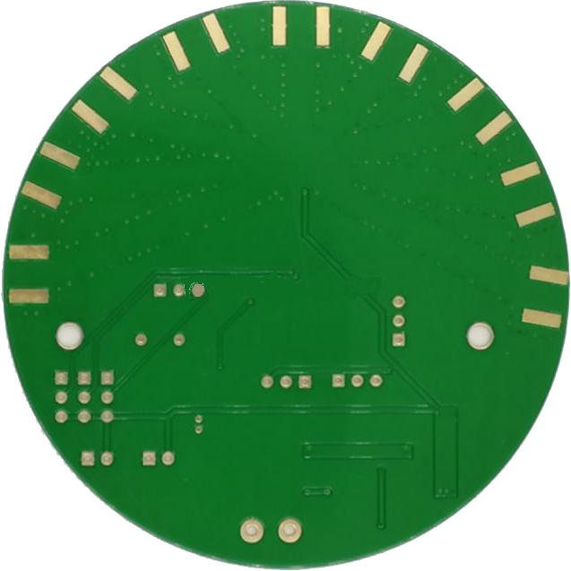
发布时间:2023-08-28 | 信息来源:遇见电路(深圳)有限公司高密度互连HDI电路板代表了印刷电路板市场增长最快的部分之一。由于HDI电路板较高的电路密度,因此设计时可以合并更细的线和空间,更小的通孔和捕获焊盘以及更高的连接焊盘密度。HDI电路板具有盲孔和埋孔,并且通常包含直径为0.006或更小的微孔。那么,HDI电路板的特点及用途都有哪些呢?
1、HDI电路板的特点
HDI电路板技术的发展为工程师带来了前所未有的设计自由和灵活性,可以根据需要在原始PCB的两侧放置更多组件,同时允许将更小的组件放置在一起。这意味着HDIPCB最终会导致更快的信号传输以及增强的信号质量。
HDI电路板被广泛用于减少产品的重量和整体尺寸,以及增强设备的电气性能;经常出现在手机、触摸屏设备、笔记本电脑、数码相机和4G网络通信中。HDI电路板在医疗设备以及各种电子飞机零部件中也很突出。
2、HDI电路板的用途
HDI电路板适用于各种行业。如上所述,您会在智能手机和平板电脑等所有类型的数字设备中找到它们,而微型化是产品有效应用的关键。您还可以在依赖电子产品的汽车,飞机和其他车辆中找到它。
高密度PCB取得巨大进展的最关键领域之一是医疗领域。医疗设备经常需要具有高传输速率的小包装,只有HDI电路板才能提供。例如,植入物需要足够小以适合人体,但是植入物中涉及的任何电子设备绝对必须有效地允许高速信号传输。此外,其他医疗设备,例如急诊室监视器、CT扫描等也可到HDI电路板。上一篇:怎么判断HDI线路板的质量下一篇:PCB多层线路板的相关知识相关资讯

专业高精密PCB电路板研发生产厂家
PCB打样加急,高频线路板,PCB多层线路板,线路板打样,FPC软板打样生产
热线:13798484718 邮箱:445752204@qq.com
