-
PCB多层线路板的相关知识
发布时间:2023-08-28 | 信息来源:遇见电路(深圳)有限公司在电子产品制造过程中,电路板是至关重要的组件。而在众多类型的电路板中,PCB多层线路板因其具有更高的性能和更低的功耗而备受关注。本文将带您了解PCB多层线路板的相关知识。
1.PCB多层线路板的定义
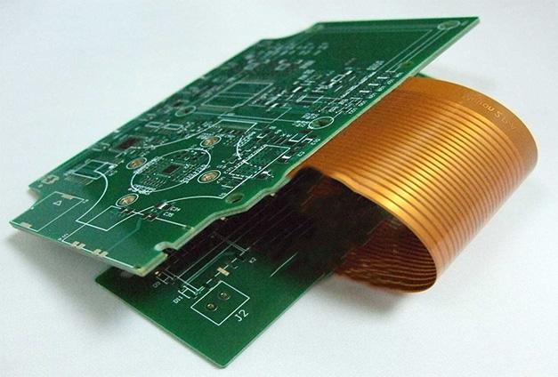
PCB多层线路板(High-Density Multi-Layer PCB)是一种具有多个内层和外层的印刷电路板。与传统的单层或双层PCB相比,PCB多层线路板具有更多的信号层和电源层,从而提高了电路板的性能和可靠性。此外,PCB多层线路板还可以通过堆叠更多的内层来实现更高的集成度,以满足不断增长的电子设备需求。
2.PCB多层线路板的技术原理
PCB多层线路板的制作过程主要包括以下几个步骤:设计、制版、光刻、蚀刻、沉积、检测等。在这个过程中,需要使用专业的软件进行电路板的设计和仿真,然后通过制版工艺将设计图案转移到光敏材料上。接下来,利用光刻和蚀刻技术将电路板上的导线和焊盘制作出来。最后,通过沉积技术在电路板上添加金属导电层,并进行最后的检测和测试。
3.PCB多层线路板的应用领域
由于其优越的性能和高度集成的特点,PCB多层线路板广泛应用于各种电子设备中,如智能手机、平板电脑、服务器、汽车电子、医疗设备等。特别是在5G通信、人工智能、物联网等领域,PCB多层线路板发挥着举足轻重的作用。
4.PCB多层线路板的未来发展趋势
随着技术的不断进步,PCB多层线路板将继续向更高性能、更低功耗的方向发展。例如,采用新型的材料和工艺可以实现更小尺寸、更高密度的线路板;同时,通过引入新的设计理念和技术手段,可以进一步提高电路板的可靠性和稳定性。此外,环保和可持续发展也将成为PCB多层线路板产业发展的重要方向。
总之,PCB多层线路板作为电子产品的核心组件,其技术和应用前景广阔。上一篇:HDI电路板的特点及用途相关资讯

专业高精密PCB电路板研发生产厂家
PCB打样加急,高频线路板,PCB多层线路板,线路板打样,FPC软板打样生产
热线:13798484718 邮箱:445752204@qq.com
