-
什么是HDI板(盲埋孔板)打样
发布时间:2023-09-13 | 信息来源:遇见电路(深圳)有限公司HDI:high Density interconnection的简称,高密度互连,非机械钻孔,微盲孔孔环在6mil以下,内外层层间布线线宽/线隙在4mil以下,焊盘直径不大于0.35mm的多层板制作方式称之为HDI电路板。
盲孔:Blind via的简称,实现内层与外层之间的连接导通
埋孔:Buried via的简称,实现内层与内层之间的连接导通
盲孔大都是直径为0.05mm~0.15mm的小孔,埋盲孔成孔方式有激光成孔,等离子蚀孔和光致成孔,通常采用激光成孔,而激光成孔又分为CO2和YAG紫外激光机(UV)。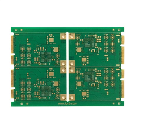
特性(Feature)
板材性能(Laminate Properties)
应用(Application)
•无卤,无锑,无红磷Tg170℃
Halogen,antimony and red phosphorous free
•优良的耐热性
Excellent thermal reliability
•优良的介电性能(Dk=4.1,Df=0.008)
Low Dk/Df
•低的Z轴热膨胀系数
Low Z-CTE
•良好的耐CAF性能
Anti-CAF capability
•服务器,交换机,基站
Server,Switch,Base station
•背板
Backplane
•高性能计算机
High performance computing
•网络通信
Network and telecom application
•高复杂度多层板
High complexity multi-layers上一篇:高频高速板的定义相关资讯

专业高精密PCB电路板研发生产厂家
PCB打样加急,高频线路板,PCB多层线路板,线路板打样,FPC软板打样生产
热线:13798484718 邮箱:445752204@qq.com
