-
什么是PCB打样?PCB线路板市场趋势如何?
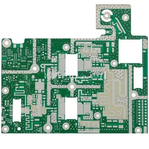
发布时间:2023-09-12 | 信息来源:遇见电路(深圳)有限公司PCB打样就是指印制电路板在批量生产前的试产主要应用为电子工程师在设计好电路?并完成PCB Layout之后向工厂进行小批量试产的过程即为PCB打样。而PCB打样的生产数量一般没有具体界线一般是工程师在产品设计未完成确认和未完成测试之前都称之为PCB打样,是一个设计与实践验证的过程。
PCB线路板整个技术市场都相比传统发生了改变,因为传统的PCB线路板密度没有现在高,现在的不仅密度高,而且刚柔结合,IC基板和HDI等新技术的兴起为智能手机和汽车应用中的高级PCB创造了巨大潜力,并推动了对PCB技术的需求。
在PCB市场中,各种技术使用了诸如刚性1-2面,标准多层板,柔性电路,刚柔结合,HDI/微孔/堆积和IC基板之类的技术。通信行业对PCB的需求不断增长,连接设备的增长以及汽车电子技术的进步为各种PCB技术创造了新的机遇。
根据有关研究表示,在未来,PCB线路板将以7.8%的复合年增长率增长,估计增长速度很快,在计算机,通信行业应用广泛。
纵观未来印制电路板市场发展趋势,将必然向高精密、高密度互联、环保型以及高频微波板方向发展,遇见电路将加强技术创新力度,主攻层数高、技术含量高、性价比高的产品开发,审时度势,使公司的技术水平更上一层楼,同时紧随印制电路板市场发展之趋势。上一篇:无信息下一篇:线路板打样注意事项相关资讯

专业高精密PCB电路板研发生产厂家
PCB打样加急,高频线路板,PCB多层线路板,线路板打样,FPC软板打样生产
热线:13798484718 邮箱:445752204@qq.com
