-
8层2阶HDIPCB板打样厂家
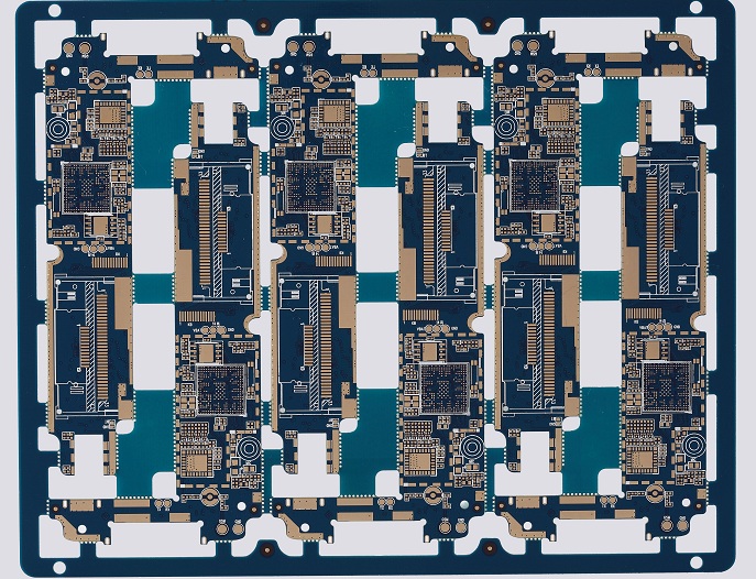
发布时间:2023-08-15 | 信息来源:遇见电路(深圳)有限公司HDI(High Density Intrerconnection)电路板的定义是指孔径在6mil以下,孔环之环径(Hole Pad)在0.25mm以下者的微导孔(Microvia),接点密度在130点/平方吋以上,布线密度于117吋/平方吋以上,线宽/间距为 3mil/3mil以下的印刷线路板。HDI线路板主要应用于手机、照相机、摄像机、笔记本电脑、上网卡、IC载板、军工、医疗等不同的领域。
8层2阶HDIPCB板打样厂家来给大家介绍下HDI线路板的优点:
1.降低成本
2.增加布线密度
3.有利于先进封装技术的使用
4.拥有更佳的电性能及信号正确性
5.可靠性较佳
6.可改善热性质
7.可改善射频干扰、电磁波干扰、静电释放
8.增加设计效率 上一篇:陶瓷PCB线路板生产工艺下一篇:PCB多层线路板的价格算法相关资讯

专业高精密PCB电路板研发生产厂家
PCB打样加急,高频线路板,PCB多层线路板,线路板打样,FPC软板打样生产
热线:13798484718 邮箱:445752204@qq.com
