-
PCB打样厂家介绍HDI盲埋孔板
发布时间:2023-08-24 | 信息来源:遇见电路(深圳)有限公司在PCB打样行业中,经常会提到“HDI盲埋孔”这个词汇。现在HDI板(盲埋孔板)打样厂家遇见就给大家科普及一下PCB打样中的“HDI盲埋孔”。
盲孔,是只在PCB板子顶层或底层其中的一层看得到,也就是说盲孔是从表面上钻,但是不钻透所有层。
埋孔,是指做在内层过孔,该孔之上、下两面都在板子的内部层,换句话说是埋在板子内部的。
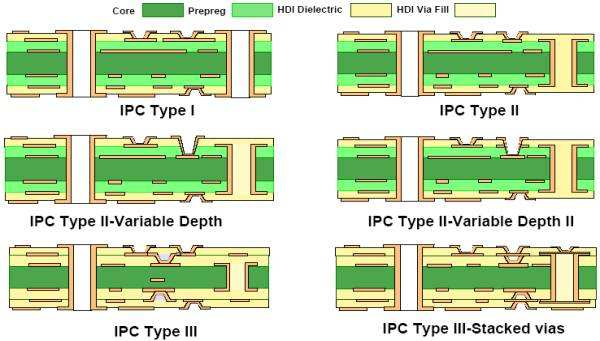
在PCB打样中,盲孔和埋孔的应用,极大地降低HDI(高密度互连)PCB的尺寸和质量,减少层数,提高电磁兼容性,增加电子产品特色,降低成本,同时也会使得设计工作更加简便快捷。

在PCB快板行业,很多企业是不愿意去做盲埋孔的,因为比较麻烦,制作工序繁多,需要专业设备,特殊工艺,时效较长,成本较高。遇见电路致力于做别人不肯做的板子。花巨资引进盲埋孔的相关设备,如激光钻孔,树脂塞孔等。现在已突破最高阶层为20层;板厚≤6.0mm;盲孔阶数1~4阶;最小孔径0.076mm。
遇见在PCB制造业中不断努力提高PCB的生产工艺,全力为客户解决技术及生产工艺难题,公司始终保持着生产高质量线路板产品的宗旨,结合精密的生产制造测试设备打造中国精密的PCB制造工厂,具有高频高速,高阶HDI线路板核心生产技术的高精密线路板生产企业。
上一篇:多层HDI板(盲埋孔板)打样介绍相关资讯

专业高精密PCB电路板研发生产厂家
PCB打样加急,高频线路板,PCB多层线路板,线路板打样,FPC软板打样生产
热线:13798484718 邮箱:445752204@qq.com
