-
HDI线路板的相关介绍
发布时间:2023-11-15 | 信息来源:遇见电路(深圳)有限公司生活在移动互联网时代,手机通讯,电脑电子对人们的影响是非常大的,这也是HDI线路板应用较大的领域,特别是进入5G,在PCB打样中对HDI线路板提出更高的需求。
线路板厂讲与传统的多层板相比,在PCB打样中,HDI线路板采用积层法制板,运用盲孔和埋孔来减少通孔的数量,节约了PCB的可布线面积,从而大幅度提高元器件密度,因而在智能手机的运用中迅速替代了原有的多层板。
HDI技术主要是对印制电路板孔径的大小、布线的宽窄、层数的高低等方面要求较高,需要多埋盲孔,呈现高密度发展。在高端服务器所需要的各种PCB产品中,主要是通讯和计算机行业占比较大,对HDI线路板需求相对较高。
电路板厂了解到,当前HDI板在国内的份额市场非常看好。服务器HDI卡、手机、多功能POS机,以及HDI安防摄像机等都大范围使用HDI高密度板。HDI线路板的市场不断向高端高层高密度方面发展,不断的影响我们的通讯事业,推动科技不断前进!
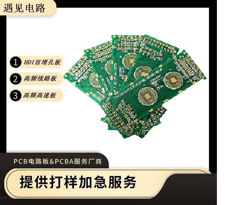
以上内容由HDI板(盲埋孔板)打样厂家遇见电路小编整理于网络分享,遇见电路是一家高精密pcb打样、pcb加急,高频线路板,高频高速板,pcb多层线路板,线路板打样、pcb阻抗板打样、hdi板(盲埋孔板)打样,fpc软板打样生产,小批量生产加工。样板最快小时速生产。
上一篇:浅析HDI线路板叠层结构图解相关资讯

专业高精密PCB电路板研发生产厂家
PCB打样加急,高频线路板,PCB多层线路板,线路板打样,FPC软板打样生产
热线:13798484718 邮箱:445752204@qq.com
